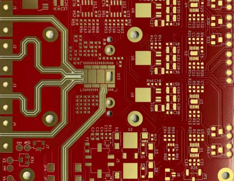
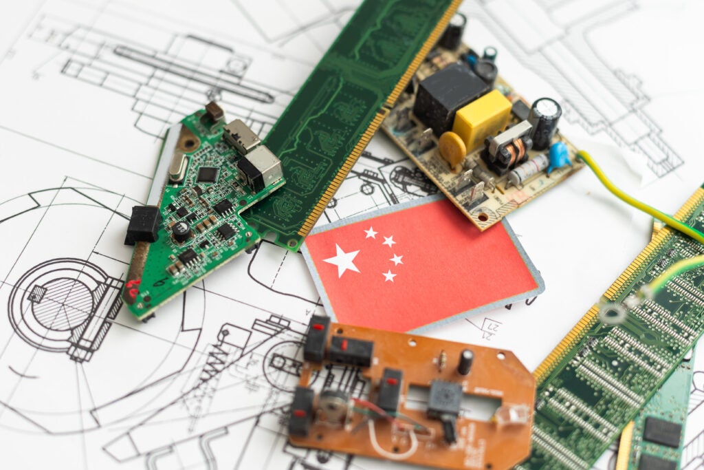
PCIe PCB Layout Guidelines: The Rules High-Speed Design Pros Follow - Pci and pcie in pcb layout design-elepcb
If you are looking for A detailed guide to PCB layout design - IBE Electronics you've came to the right web. We have 35 Images about A detailed guide to PCB layout design - IBE Electronics like High Speed Pcb Layout Guidelines - Design Talk, Advanced PCB Layout Course - Practice on PCIE during lesson 2 and also impedance matching - PCB design for high-frequency differential lanes. Here it is:
A Detailed Guide To PCB Layout Design - IBE Electronics
 www.pcbaaa.com
A detailed guide to PCB layout design - IBE Electronics
Getting Started With RF PCB Layout Guidelines
 www.hemeixinpcb.com
Getting Started With RF PCB Layout Guidelines
PCB Layout Guidelines | Design Rules & Requirements | Tips
 www.wellpcb.com
PCB Layout Guidelines | Design Rules & Requirements | Tips
Best PCB Layout Design Guide For Prototyping
Best PCB Layout Design Guide For Prototyping
PCB Layout Guidelines | Design Rules & Requirements | Tips
 www.wellpcb.com
PCB Layout Guidelines | Design Rules & Requirements | Tips
PCB Layout Guidelines | Design Rules & Requirements | Tips
 www.wellpcb.com
PCB Layout Guidelines | Design Rules & Requirements | Tips
PCB Design And Pinout For PCIe Edge Cards
 resources.altium.com
PCB Design and Pinout For PCIe Edge Cards
Complete Guide To PCB Layout Design: Tips, Basics, & Guidelines
 sfxpcb.com
Complete Guide to PCB Layout Design: Tips, Basics, & Guidelines
PCIe Routing Guidelines: Overview | EMA Design Automation
 www.ema-eda.com
PCIe Routing Guidelines: Overview | EMA Design Automation
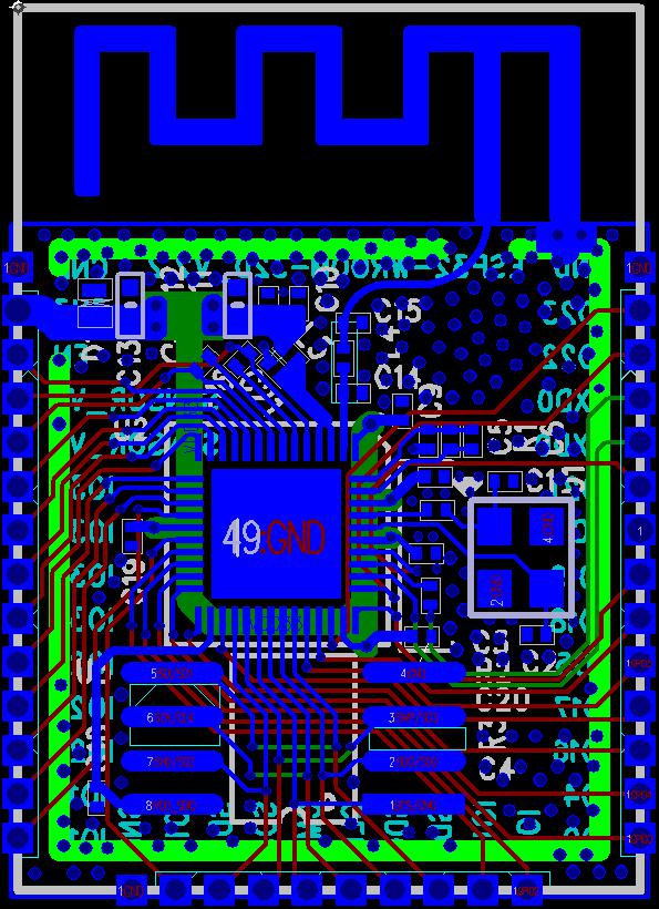
PCI And PCIe In PCB Layout Design-ELEPCB - ELEPCB
 www.elepcb.com
PCI and PCIe in PCB Layout Design-ELEPCB - ELEPCB
Advanced PCB Layout Course - Practice On PCIE During Lesson 2
 fedevel.com
Advanced PCB Layout Course - Practice on PCIE during lesson 2
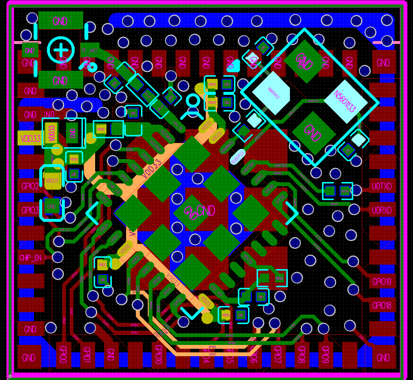
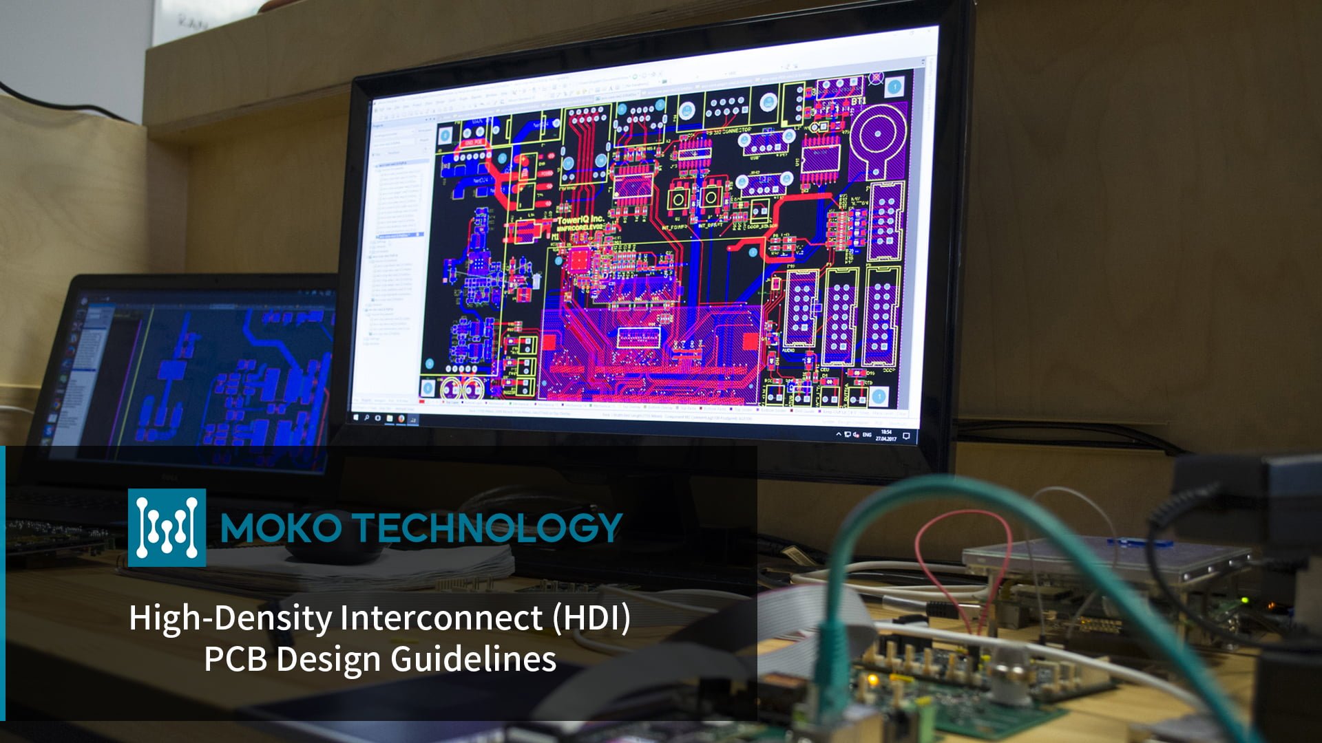
PCB Layout Design - ESP32-C3 - — ESP Hardware Design Guidelines Latest
 docs.espressif.com
PCB Layout Design - ESP32-C3 - — ESP Hardware Design Guidelines latest ...
PCB Layout Design - ESP32 - — ESP Hardware Design Guidelines Latest
 docs.espressif.com
PCB Layout Design - ESP32 - — ESP Hardware Design Guidelines latest ...
PCB Layout Guidelines | Design Rules & Requirements | Tips
 www.wellpcb.com
PCB Layout Guidelines | Design Rules & Requirements | Tips
PCIe Routing Guidelines & Best Practices - Free Online PCB CAD Library
 www.ultralibrarian.com
PCIe Routing Guidelines & Best Practices - Free Online PCB CAD Library
Pcb Component Layout _ Pcb Layout Guide – CBYIBF
 wnduk.com
Pcb Component Layout _ Pcb Layout Guide – CBYIBF
High Speed Pcb Layout Guidelines - Design Talk
 design.udlvirtual.edu.pe
High Speed Pcb Layout Guidelines - Design Talk
Pcb Design And Layout Services » Hackatronic
 hackatronic.com
pcb design and layout services » Hackatronic
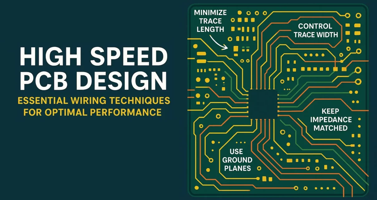
High Speed PCB Design Routing And Layer Stackup Techniques
 www.viasion.com
High Speed PCB Design Routing and Layer Stackup Techniques
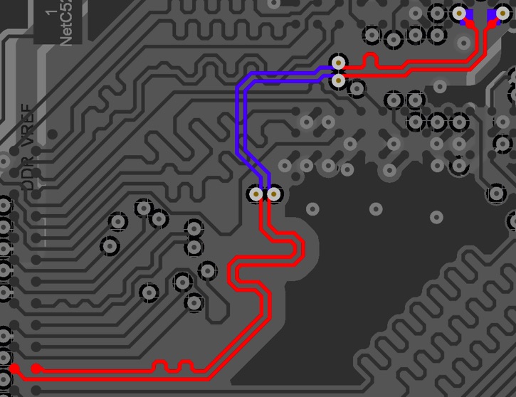
PCIe & DDR Layout Guidelines
 www.linkedin.com
PCIe & DDR Layout Guidelines
PCIe Routing Guidelines: Overview | EMA Design Automation
 www.ema-eda.com
PCIe Routing Guidelines: Overview | EMA Design Automation
What Is High-Speed PCB Design And Guidelines? | Viasion
 www.viasion.com
What is High-Speed PCB Design and Guidelines? | Viasion
High Speed Pcb Design Guidelines Ppt - Design Talk
 design.udlvirtual.edu.pe
High Speed Pcb Design Guidelines Ppt - Design Talk
PCIe Layout And Routing Guidelines | Blog | Altium Designer
 resources.altium.com
PCIe Layout and Routing Guidelines | Blog | Altium Designer
PCB Layout Guidelines For High Speed Applications
 www.linkedin.com
PCB Layout Guidelines For High Speed Applications
Impedance Matching - PCB Design For High-frequency Differential Lanes
 electronics.stackexchange.com
impedance matching - PCB design for high-frequency differential lanes ...
High Speed Pcb Layout Guidelines - Design Talk
 design.udlvirtual.edu.pe
High Speed Pcb Layout Guidelines - Design Talk
PCB Layout Guidelines | Design Rules & Requirements | Tips
 www.wellpcb.com
PCB Layout Guidelines | Design Rules & Requirements | Tips
High Speed Pcb Design Guidelines Ppt - Design Talk
 design.udlvirtual.edu.pe
High Speed Pcb Design Guidelines Ppt - Design Talk
PCB Layout Rules For PCIE, SATA, LAN, LVDS, USB, SDVO,
 www.fedevel.com
PCB layout rules for PCIE, SATA, LAN, LVDS, USB, SDVO,
PCI And PCIe In PCB Layout Design-ELEPCB - ELEPCB
 www.elepcb.com
PCI and PCIe in PCB Layout Design-ELEPCB - ELEPCB
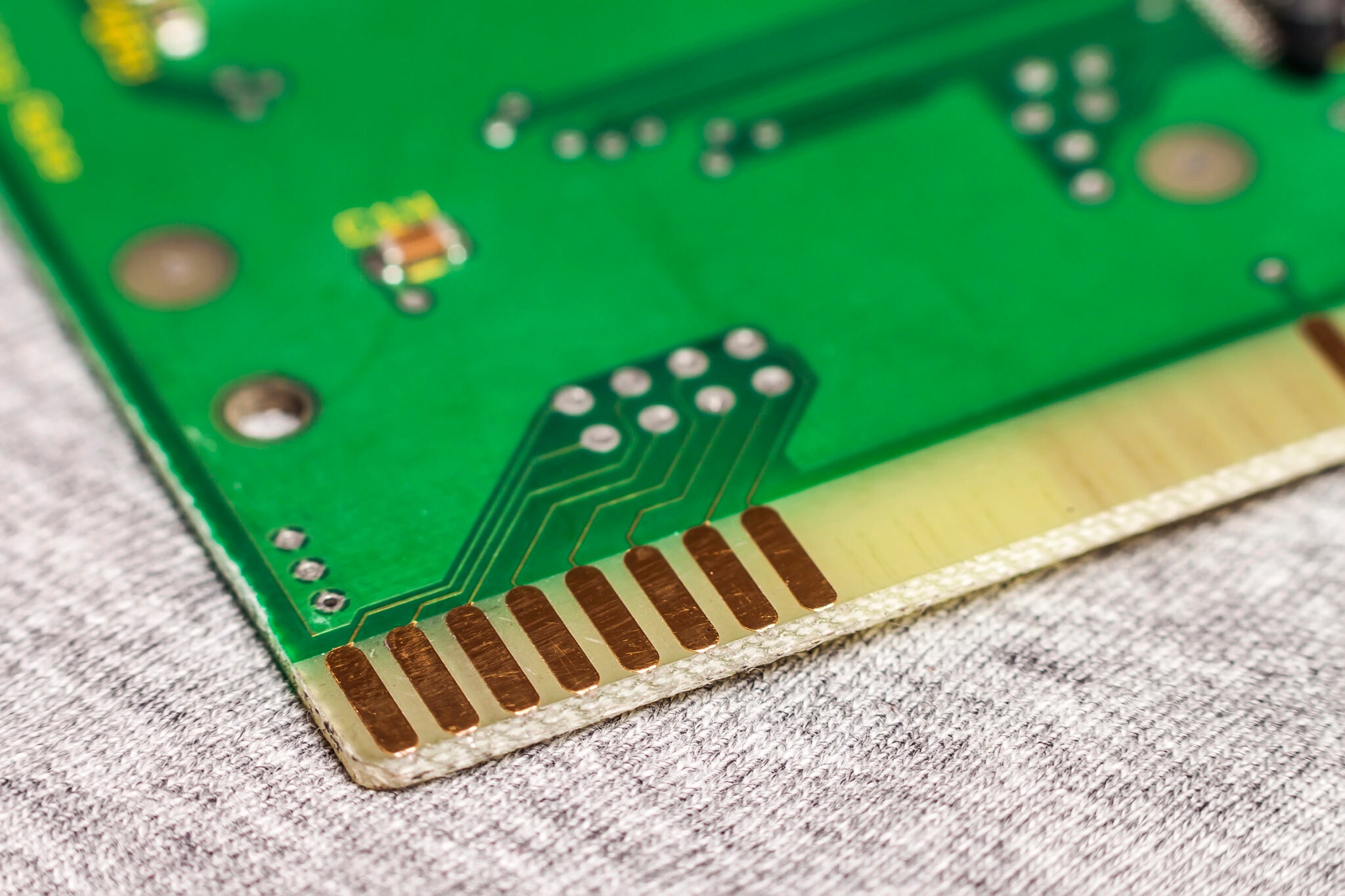
How To Design A PCB Layout
 hilelectronic.com
How to Design a PCB Layout
PCIe Routing Guidelines: Overview | EMA Design Automation
 www.ema-eda.com
PCIe Routing Guidelines: Overview | EMA Design Automation
Main Design Guidelines & Layout Rules On High Speed PCB
 www.integrasources.com
Main Design Guidelines & Layout Rules on High Speed PCB
PCI And PCIe In PCB Layout Design-ELEPCB - ELEPCB
 www.elepcb.com
PCI and PCIe in PCB Layout Design-ELEPCB - ELEPCB
Pcb layout guidelines. Pci and pcie in pcb layout design-elepcb. Main design guidelines & layout rules on high speed pcb